Hi, I am using an X2 with a LSM303DLH from pololu.
Modifying the pololu code on the X2 resource page. As far as i can tell the code is getting stuck in the
i2c_start();
I have set PORTD to turn on before i2c_start(); and turn off once i2c_start(); returns.
I am getting close to the expected voltages on the 1.8 and 3v output pins and have had the same problem with other i2c components.
Scoping what the pins i have identified as PC0 I get 1.92v out when i set it to a an output and drive high.
PC1 I get 1.16v.
LCD is not connected. and all lcd code has been removed. However LCD code was modified for 4 wire anyway.
Identified PC0 and PC1 by toggling while in a loop with a delay and I am confident they are correct and they are in the 4th row of two pins on the lcd plug from the power button.
I think it gets stuck on this line
while (!(TWCR & (1 << TWINT)));
And i suspect it is due to the low voltages the i2c components are not responding.
int main()
{
	DDRC = 0;                              // all inputs
	PORTC = (1 << PC1) | (1 << PC0); // enable pull-ups on SDA and SCL, respectively
	//end test
	TWSR = 0;  // clear bit-rate prescale bits
	TWBR = 17; // produces an SCL frequency of 400 kHz with a 20 MHz CPU clock speed

	DDRD=0xff;
	PORTD=0xff;
//	clear();

	//enable accelerometer
	i2c_start();

	PORTD=0x00;
	i2c_write_byte(0x30); // write acc
	i2c_write_byte(0x20); // CTRL_REG1_A
	i2c_write_byte(0x27); // normal power mode, 50 Hz data rate, all axes enabled
	i2c_stop();

	//enable magnetometer
	i2c_start();
	i2c_write_byte(0x3C); // write mag
	i2c_write_byte(0x02); // MR_REG_M
	i2c_write_byte(0x00); // continuous conversion mode
	i2c_stop();

	while(1);

}

void i2c_start() {
	TWCR = (1 << TWINT) | (1 << TWSTA) | (1 << TWEN); // send start condition
	while (!(TWCR & (1 << TWINT)));
}

void i2c_write_byte(char byte) {
	TWDR = byte;
	TWCR = (1 << TWINT) | (1 << TWEN); // start address transmission
	while (!(TWCR & (1 << TWINT)));
}

char i2c_read_byte() {
	TWCR = (1 << TWINT) | (1 << TWEA) | (1 << TWEN); // start data reception, transmit ACK
	while (!(TWCR & (1 << TWINT)));
	return TWDR;
}
I’ll take a closer look at your post in the morning, but I just wanted to mention now that if you are not seeing 5 V on your digital output when you drive it high, something is very wrong. Do you have anything connected to PC0 and PC1? If not, are you sure you’re measuring them right? Do you see 5 V if you drive some other digital output high, such as A0? Can you post the code you used to set PC0 and PC1 high?
Hi Ben,
I was using a Digital oscilloscope and if i use a portD pin I have 5v compared to ground when I make it an output and drive send it high. Nothing else of my own is connected to the PC0 and PC1 however there is the LCD and pushbutton switch as per the X2 schematic.
I will see if I can get my hands on a second X2 later from another project to test if the voltage is as expected for the second one.
code to turn on the pins was
int main()
{
	DDRC=0xff;
	PORTC=(1<<PC0)|(1<<PC1);
	while(1);
}
EDIT: just used a digital multimeter with the same code on a different x2. voltage looks like very close to 5v. I will later when I have access to both to try the other x2 see if the i2c works. Still would appreciate if you check the code for any major problems.
Is it possible that you forgot to make the PC0 and PC1 pins outputs in your earlier tests and rather were just enabling the internal pull-ups. If so, that would have effectively produced a voltage divider (there are pull downs on those lines: 1k + LED on PC0 and 10k on PC1). With the internal pull-up enabled (which is typically around 30k on the X2’s ATmega1284, if I remember right), the voltage on PC1 would be approximately 1.2 V, and the voltage on PC0 would be very close to the yellow LED’s forward voltage drop of 2 V. This seems to be pretty close to what you observed.
Now that I’ve looked at this more closely, I do not think that hardware I2C will work well on the X2 in it’s default state: since the I2C/TWI protocol use pull-ups to achieve logical highs rather than driving the lines high, the pull-downs on the SCL and SDA pins will keep the voltages too low. I think you have basically have two options:
Use software I2C on free pins (port A or port D). Implementing master I2C in software is fairly easy, and there are probably a number of libraries for this already written for the AVR. If not, the wikipedia page on I2C has a sample C code for bit-banging the I2C master protocol that will mostly just work on the X2 (you just have to write the functions that do the timing and that set/clear SDA and SCL).
If you’re comfortable giving up the yellow LED on PC0 and the PC1 pushbutton, you can cut the pull-down traces on these lines or desolder the pull-down resistors. Note that you might actually be able to leave the 10k pushbutton pull-down on PC1 if you use a strong enough I2C pull-up (e.g. 1k - 4k) and a maybe slower I2C frequency, but I think the 1k LED pull-down is just going to be too strong to reasonably overcome.
It is theoretically possible for it to have been an input and enabling internal pullups.
Am I right in assuming the long line of smd resistors near the SW2 and D9 belong with these. Just trying to determine the best place to cut the track as I have never used the LED’s or pushbuttons. Removing SW2 should Open circuit the current load on PC0 allowing for a pullup to the near 5v required for the open drain of the i2c. I cot track with my limited equipment here the correct 10k smd for the switch. Removing the switch may help.
It seems like you could help confirm that theory by running the code you posted above on the original Orangutan to see if you now get closer to 5 V on both of those pins
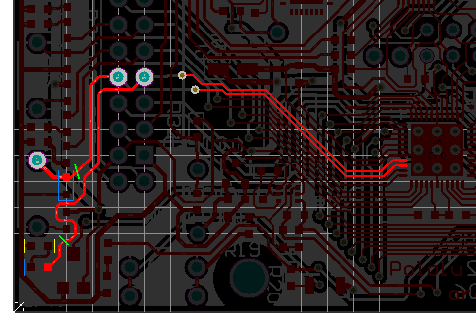
The following picture shows the top copper layer of the lower left corner of the X2, with the PC0 and PC1 traces highlighted:
The blue rectangles show the locations of the relevant resistors, and the yellow rectangle shows the location of the yellow LED. You can desolder the two resistors represented by the blue rectangles, or you can cut the traces between the LCD header and the pull-down resistors. The green lines show the two places where it might be easiest to cut the traces (it’s kind of tight in that area with the LCD connector and all of the parts around it). Note that PC1 resistor has another resistor right below it, so it is the second resistor in the long, vertical chain or resistors if you start counting from the bottom. Please let me know if you have any questions or if anything is unclear.
Once you make the board modifications, can you enable the internal pull-ups on PC0 and PC1 and see if the voltage goes to 5 V?